Why is lead-free PCBs best suited for your projects and products?
- info632049
- Feb 27
- 3 min read
Choosing the right printed circuit board (PCB) is crucial for electronics designers and professionals working across industries like automation, communication, consumer electronics, solar, and electric vehicles (EV). One key decision is whether to use lead-free PCBs or traditional lead-based ones. Lead-free PCBs have become the preferred choice for many projects and products, offering benefits that align with modern environmental standards, reliability needs, and performance expectations.
This post explores why lead-free PCBs are best suited for your designs, highlighting practical advantages and industry examples.

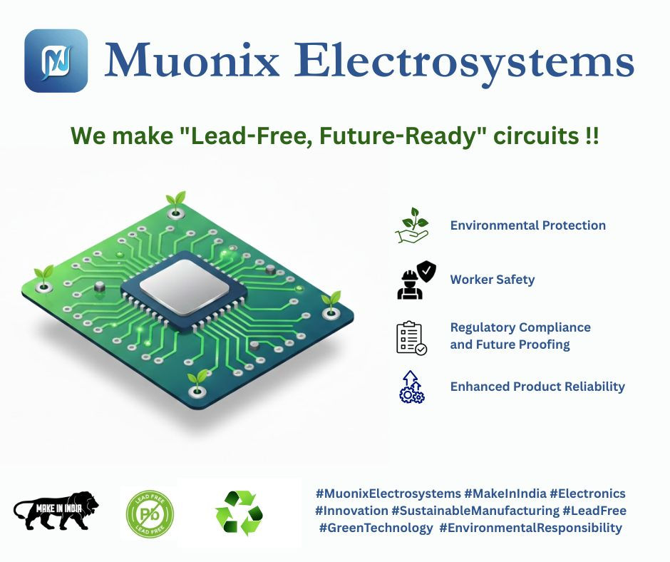
Environmental and Regulatory Compliance
Lead is a toxic heavy metal that poses health and environmental risks. Many countries have introduced strict regulations limiting or banning lead in electronics manufacturing. The Restriction of Hazardous Substances Directive (RoHS) in the European Union is a prime example, requiring manufacturers to reduce or eliminate lead in PCBs.
Using lead-free PCBs ensures your projects comply with these regulations, avoiding legal issues and potential fines. It also supports corporate responsibility goals by reducing hazardous waste and environmental contamination.
Improved Reliability and Performance
Lead-free solder alloys, commonly made from tin, silver, and copper, offer higher melting points compared to traditional lead-based solders. This characteristic improves the thermal stability of PCBs, which is critical in demanding applications such as:
Automation systems that operate continuously under varying temperatures
Communication devices exposed to fluctuating environmental conditions
Solar power electronics that face high heat from sunlight exposure
Electric vehicles (EV) where thermal management is vital for battery and motor control systems
The higher melting point reduces the risk of solder joint failure during operation, enhancing the overall reliability of your product.
Health and Safety Benefits
Lead exposure can cause serious health problems for workers involved in PCB assembly and manufacturing. By choosing lead-free PCBs, companies protect their workforce from lead poisoning risks. This is especially important in factories producing relays and other components where soldering is frequent.
Moreover, lead-free PCBs reduce the risk of lead contamination in consumer electronics, making devices safer for end-users, including children and vulnerable populations.
Compatibility with Modern Manufacturing Processes
Modern electronics manufacturing increasingly favors lead-free processes. Automated soldering equipment, such as reflow ovens and wave soldering machines, are optimized for lead-free solder alloys. This compatibility ensures smoother production runs, fewer defects, and better yields.
For example, in the production of relays used in automation and communication systems, lead-free PCBs allow for precise soldering without compromising component integrity. This leads to consistent product quality and reduced rework costs.
Cost Considerations and Long-Term Savings
While lead-free solder materials can be slightly more expensive than lead-based ones, the overall cost difference has narrowed significantly. The benefits of lead-free PCBs often outweigh the initial investment:
Lower risk of product recalls due to regulatory non-compliance
Reduced health and safety liabilities
Enhanced product lifespan and reliability, decreasing warranty claims
Access to markets with strict environmental standards
In sectors like consumer electronics and EV manufacturing, where product safety and durability are paramount, these savings add up.
Supporting Sustainability Goals
Sustainability is a growing priority for companies and consumers alike. Lead-free PCBs contribute to greener electronics by reducing hazardous materials in the supply chain. This aligns with the increasing demand for eco-friendly products in solar energy systems and electric vehicles.
Designers can highlight the use of lead-free PCBs as part of their product’s environmental credentials, appealing to environmentally conscious customers and stakeholders.
Practical Examples Across Industries
Automation: Factories implementing lead-free PCBs in control relays experience fewer maintenance issues due to improved solder joint strength.
Communication: Telecom equipment manufacturers use lead-free PCBs to meet global standards and ensure device longevity in harsh environments.
Consumer Electronics: Smartphones and wearable devices rely on lead-free PCBs to comply with regulations and reduce toxic waste.
Solar: Inverters and monitoring systems benefit from lead-free PCBs that withstand high temperatures and outdoor conditions.
EV: Battery management systems and motor controllers use lead-free PCBs to improve thermal performance and safety.
Final Thoughts
Lead-free PCBs offer clear advantages for electronics designers and professionals working on projects in automation, communication, consumer electronics, solar, and EV sectors. They meet regulatory requirements, improve product reliability, protect health, and support sustainability goals.
Choosing lead-free PCBs is a practical step toward building safer, more durable, and environmentally responsible products. As regulations tighten and consumer expectations rise, adopting lead-free technology will keep your designs competitive and compliant.


Comments